Printed circuit boards are the unsung heroes behind our modern technological world. Be it smartphones or medical devices, a PCB forms the backbone of most electronic devices. The question now is how these intricate and crucial parts are created. Let us delve into the important details Instagram bio for boys during the fascinating process of manufacturing a printed circuit board in these steps.
1. Design and Layout
The journey of PCB manufacturing begins with designing. Engineers use specialized software like Eagle, Altium Designer, or KiCad to create a detailed blueprint of the board. This design includes the placement of components, the routing of electrical connections, and the definition of various layers. It’s akin to an architect drafting the blueprints for a building. Every detail must be meticulously planned to ensure functionality and reliability.
2. Printing the Design
Now that the design is ready, it’s time to give body to the design. It starts with a print of the design on a laminate board made of usual fibreglass. The design is printed on it through a special printer. This printer uses special ink made from conductive materials like copper. This process, called photo-plotting, transfers the intricate design onto the board with precision accurately.
3. Creating the Substrate
The substrate is usually a composite epoxy or fibreglass material that forms the base of the printed circuit board. You can think of it like the foundation of a house, to which everything else is fastened. Typically, the substrate is covered on both sides with a thin layer of copper. This copper will soon become the conductive pathways that interconnect the different components.
4. Drilling
Drilling is a vital process where small holes, known as vias, are created to help in electronic interlinking between the different layers of the PCB. These holes are made using a precision drill, generally controlled by computer numerical control, with great accuracy. These vias will serve as the pathways for the electrical signals to communicate across the board.
5. Plating and Copper Deposition
Subsequently, the board is electroless copper-plated. The board is immersed in a chemical bath, and over all the exposed places, including the interiors of the drilled holes, a thin layer of copper is deposited. The vias are thus made conductive for use in electrical connectivity in subsequent steps.
6. Imaging the Pattern
The next step involves transferring the PCB design onto the copper-clad board. This is achieved through a process called photolithography. A photosensitive film, called a photoresist, is applied to the board. The design is then projected onto the board using ultraviolet (UV) light. The areas exposed to the UV light harden, while the unexposed areas remain soft and are washed away. This leaves behind the desired copper pattern on the board.
7. Etching
Etching is a crucial step where the excess copper is removed, leaving only the desired copper traces. The board is immersed in an etching solution, often made of ferric chloride or ammonium persulfate. This solution dissolves the unwanted copper, revealing the intricate network of pathways that will carry electrical signals.
8. Solder Mask Application
To protect the delicate copper traces and prevent short circuits, a solder mask is applied to the board. This mask is a protective layer that covers everything except the areas where components will be soldered. It not only safeguards the copper but also gives the PCB its distinctive green (or sometimes other colours) appearance.
9. Silkscreen Printing
The silkscreen printing process adds the final touches to the PCB by printing vital information on the board’s surface. Component labels, logos, and other markings that make the assembly easier and facilitate troubleshooting are stamped in. /  It’s like the signposts and labels on a roadmap that guide engineers during the process of assembly.
10. Surface Finish
A surface finish is administered not only to ensure good solderability but also to prevent the oxidation of copper. Common finishes include HASL, ENIG, and OSP. Each finish has its advantages for covering different requirements and applications.
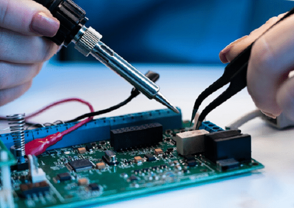
11. Assembly and Testing
With the board ready, assembling the components, which includes placing and soldering resisters, capacitors, and integrated circuits on the board is the next course of action. These positions correctly with a pick-and-place machine, an automated machine, before reflow oven or wave soldering machines fix them in place.
After the successful assembly of a printed circuit board, it undergoes rigorous testing to ensure that it will turn out to be precisely what one wants. AOI, X-ray inspection, and functional testing are adopted to point out any defects or problems. It is something on the order of what one might consider with the final quality control check of some product on its way to the store shelves.
12. Final Inspection and Quality Control
Before the PCB is shipped, it undergoes a final inspection and quality control process. This ensures that the board meets all specifications and standards. Any defects or deviations are addressed, ensuring that only the highest quality boards make it to the end-users.
Conclusion
The process of PCB manufacturing has many wonders brought into existence by modern engineering. It combines art and science to give the backbone of our technological world. Now, everything from design to final inspection plays a crucial role in bringing about a final product that is both reliable and functional. Someday when you turn on your smartphone or any other electronic device, remember the intricate journey of the printed circuit board that makes it all come to life.